
Throughout my academic career at Cambridge and my time in smart materials research, I have constantly found myself in awe of how much our entire modern computing infrastructure relies on the physical integrity of a single material. When we talk about silicon wafer composition, it is easy to get bogged down in abstract metrics like parts-per-billion purity or bandgap energies. But in practice, working with silicon at the nanoscale feels like trying to build a perfectly level skyscraper on top of a shifting foundation; if the base layer isn’t pristine, everything above it will eventually fail.
Early in my doctoral studies, I remember analyzing crystal defect densities under high-resolution imaging, and it struck me how a single unwanted trace element could derail an entire batch of micro-components. Purity is not just a commercial buzzword; it is the absolute baseline for predictable electronic behavior.
As we push semiconductor architectures toward increasingly dense layouts and advanced packaging, our control over every single atom within that wafer becomes our greatest asset. Understanding the interplay of crystal growth, dopant concentration, and surface integrity is what bridges the gap between raw chemical synthesis and world-changing technology.
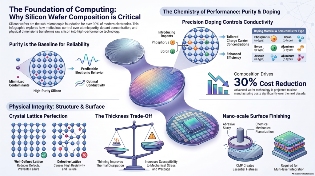
Silicon semiconductor wafer composition is vital in semiconductor manufacturing because it directly impacts device performance, efficiency, and reliability. High-purity silicon minimizes contaminants, enhancing conductivity and overall functionality. Doping materials further tailor electrical properties, improving charge carrier concentrations essential for ideal device operation. The crystal structure and surface finish also play significant roles in determining wafer quality. Understanding these factors can help you appreciate the complexities of semiconductor production, leading to more informed decisions in technology applications.
KEY TAKEAWAYS
- High silicon purity minimizes contaminants, ensuring optimal performance and reliability of semiconductor devices.
- Effective doping levels tailor electrical properties, enhancing charge carrier concentrations critical for device efficiency.
- A well-defined crystal structure reduces defects, improving conductivity and overall wafer quality.
- Wafer thickness and surface finish directly impact electrical characteristics and mechanical integrity, affecting performance.
- Sustainable manufacturing practices in wafer production enhance durability, reduce environmental impact, and align with global sustainability goals.
THE IMPORTANCE OF SILICON PURITY IN WAFER PRODUCTION
When producing silicon wafers, the purity of silicon is vital because even minor impurities can greatly impact the performance of semiconductor devices. In the simplest terms, a silicon wafer is a very pure, crystalline disc of semiconductor material, typically silicon. These wafers form the substrates upon which microchips are constructed through meticulously layering nanoscale electric components.
To achieve the highest purity standards, you must select high-quality silicon sources, such as electronic-grade silicon, which minimizes contaminants.
The production process demands rigorous control and monitoring to guarantee that any impurities are kept to an absolute minimum.
Techniques like zone refining and chemical vapor deposition can enhance purity levels, allowing you to meet the stringent requirements of advanced semiconductor applications. The effectiveness of dopants in semiconductor manufacturing boron phosphorus also depends on maintaining high-purity silicon, as impurities can interfere with the controlled electrical properties required for reliable semiconductor performance. By adhering to established purity standards, you not only improve device reliability but also maximize efficiency and performance.
By adhering to established purity standards, you not only improve device reliability but also maximize efficiency and performance.
In this competitive landscape, prioritizing silicon purity is essential for maintaining a technological edge.
What Types of Doping Materials Improve Semiconductor Performance?
When optimizing semiconductor performance, the choice of doping materials is essential. A silicon wafer is a thin, flat piece of high-purity silicon that is typically used as a substrate for the manufacture of integrated circuits (ICs), semiconductors, and other electronic devices. The wafer is sliced from a single crystal of silicon, which is grown using a method called Czochralski (CZ) crystal growth. The process results in a large monocrystalline silicon boule, which is then sliced into thin wafers of varying thickness, diameter, and purity.
Common dopants like phosphorus and boron greatly enhance electrical conductivity by altering charge carrier concentration.
Understanding their specific roles helps you maximize device efficiency and functionality.
Common Doping Materials
Doping materials play an essential role in enhancing semiconductor performance by altering electrical properties and conductivity. Your choice of doping materials considerably impacts the effectiveness of semiconductor devices. Here are some common doping materials utilized in the industry:
| Doping Material | Type of Semiconductor |
| Phosphorus | n-type |
| Boron | p-type |
| Arsenic | n-type |
| Aluminum | p-type |
Utilizing advanced doping techniques, you can optimize material selection to achieve desired electrical characteristics. Each doping material contributes unique attributes, influencing the overall performance of the semiconductor. By understanding these options, you empower yourself to design more efficient and powerful electronic components.
Impact on Electrical Conductivity
While you might consider various factors influencing semiconductor performance, the choice of doping materials greatly enhances electrical conductivity.
Doping introduces specific impurities into silicon, considerably altering its electrical properties. For instance, elements like phosphorus and boron create n-type and p-type semiconductors, respectively, maximizing charge carrier concentrations.
This controlled manipulation leads to conductivity variations, allowing for fine-tuning of the semiconductor’s response to electric fields. The precision of doping levels directly correlates with the efficiency of electronic devices; even minor adjustments can yield substantial performance improvements. In semiconductor fabrication, these dopants serve as the active ingredient that modifies the electrical behavior of silicon, enabling precise control over conductivity and device performance. This controlled manipulation leads to conductivity variations, allowing for fine-tuning of the semiconductor’s response to electric fields.
By selecting ideal doping materials, you empower the semiconductor to achieve superior conductivity, ensuring the device operates at peak efficiency and reliability.
The right doping strategy is essential for advancing semiconductor technology.
Role in Device Performance
The choice of doping materials greatly influences semiconductor performance, as specific elements enhance charge carrier mobility and overall efficiency.
For instance, phosphorus and boron are commonly used dopants that optimize n-type and p-type semiconductors, respectively. These doping techniques are also fundamental in producing lithium-ion battery active materials, where precisely controlled electrical properties contribute to improved energy storage, charging efficiency, and overall battery performance. These materials not only improve conductivity but also contribute to device longevity by minimizing thermal instability.
Additionally, incorporating elements like germanium can further enhance performance stability, facilitating better charge transport.
Shift metals, such as titanium and nickel, may also enhance specific attributes, leading to improved thermal and electrical properties.
Selecting the right doping materials is essential, as it ultimately determines the operational efficiency and reliability of your semiconductor devices in demanding applications.
How Crystal Structure Affects Silicon Wafer Quality
Crystal structure plays a critical role in determining the quality of silicon wafers, as it directly influences electrical properties and defect density. A well-defined lattice structure is essential for peak conductivity and performance in semiconductor devices.
When crystal defects occur—such as vacancies or dislocations—they disrupt the uniformity of this lattice, leading to increased resistivity and degraded electrical characteristics. You’ll find that high-quality wafers exhibit minimal crystal defects, ensuring a more reliable and efficient semiconductor performance.
WAFER THICKNESS AND DEVICE IMPACT
From a materials engineering standpoint, managing physical trade-offs is where the real work happens in the lab. When you examine wafer thickness, crystal orientation, and mechanical finishing, you are always walking a tightrope between structural durability and functional performance. Thinning a wafer can drastically improve thermal dissipation and allow for tight, multi-chip integration, but it also leaves the substrate far more susceptible to residual stress and warpage, a challenge that research teams around the world are actively trying to solve using dynamic modeling and advanced numerical analysis.
Similarly, refining the surface finish isn’t just about making a disc shiny; it’s an exercise in interfacial chemistry. When applying chemical-mechanical planarization, every nanometer of material removed changes how dielectric layers and metal contacts interact down the line.
In my own work with surface functionalization and nanostructures, I’ve seen how subtle variations in chemical etching can mean the difference between a pristine conductive interface and a high-defect zone prone to premature thermal failure. Master these surface dynamics, and you unlock the true physical potential of the underlying silicon substrate.
As you consider the impact of wafer thickness on semiconductor devices, it’s vital to recognize that variations in thickness can greatly influence performance parameters.
Achieving ideal wafer uniformity is essential; even slight thickness variation can lead to inconsistencies in electrical characteristics, ultimately affecting device reliability and efficiency. A thinner wafer may enhance performance in certain applications but can also compromise mechanical integrity, leading to higher susceptibility to defects.
Conversely, thicker wafers can offer robustness but may introduce challenges in thermal management and packing density. Understanding these trade-offs enables you to tailor wafer specifications precisely to meet device requirements, ensuring that you maximize performance while maintaining the integrity and longevity of your semiconductor products.
The Influence of Surface Finish on Wafer Efficiency
Surface finish plays a vital role in determining wafer efficiency, directly impacting various performance metrics in semiconductor devices. The quality of the surface texture is influenced by the chosen finish methods, which can enhance or degrade electrical properties. By fine-tuning these methods, you can markedly improve yield and reliability.
| Finish Method | Surface Texture Impact |
| Chemical Etching | Smooth, uniform surface |
| Mechanical Polishing | Reduced defects, improved conductivity |
| Chemical Mechanical Planarization | Enhanced flatness, superior device performance |
Selecting the appropriate finish method is essential for achieving ideal wafer efficiency. With a refined surface texture, you’ll enable better device performance, reduce defects, and ultimately drive advancements in semiconductor manufacturing.
How Wafer Composition Affects Manufacturing Costs
Understanding how wafer composition influences manufacturing costs is essential for optimizing production efficiency. The materials you choose directly impact not only wafer cost but also the overall effectiveness of your processes.
Selecting higher-quality silicon can greatly reduce defects, leading to lower rejection rates and enhanced yields.
- Increased yield translates to higher profits.
- Reduced defects minimize costly rework.
- Improved reliability fosters customer satisfaction.
- Higher-quality materials can command premium prices.
- Efficient manufacturing processes boost competitive advantage.
Future Trends in Silicon Wafer Composition and Technology
As you explore future trends in silicon wafer composition, you’ll notice a shift towards enhanced material properties that improve performance and efficiency. Silicon wafers are the basic raw material from which transistors, integrated circuits, memory chips, microprocessors and various other semiconductor devices are made, for use in electronics, familiar to us in everyday use. Wafers are made from ultra pure silicon, crystallized by the Czochralski or Float Zone methods, into single crystal ingots. These ingots are sliced into thin wafers, then lapped, etched, polished and cleaned, to become the purest, flattest, smoothest and cleanest objects possible. Only such perfections can yields the billions of submicroscopic transistors that make up modern semiconductor devices.
Additionally, eco-friendly manufacturing processes are gaining traction, driven by industry demands for sustainability.
These advancements not only optimize functionality but also align with global efforts to reduce environmental impact.
Enhanced Material Properties
While the fundamental role of silicon wafers in semiconductor technology remains unchanged, ongoing advancements in material composition are set to enhance their properties considerably.
You’ll witness improved material durability and thermal stability through innovative techniques, ultimately leading to superior performance in electronic devices.
- Increased operational efficiency
- Enhanced reliability under extreme conditions
- Longer lifespan of semiconductor components
- Superior heat resistance for high-performance applications
- Reduced risk of failure in critical systems
These enhancements empower manufacturers to push the boundaries of technology, creating powerful devices that dominate the market.
As you embrace these advancements, you’ll position yourself at the forefront of an ever-evolving industry, capable of delivering unparalleled solutions that meet the demands of tomorrow’s technology landscape.
Eco-Friendly Manufacturing Processes
With increasing environmental concerns driving innovation, manufacturers are now prioritizing eco-friendly processes in silicon wafer production. Implementing sustainable practices not only meets regulatory demands but also enhances market competitiveness.
By adopting green chemistry principles, you can minimize toxic waste and reduce energy consumption throughout the manufacturing cycle. Techniques like using biodegradable solvents and recycled materials are gaining traction, ensuring that silicon wafers are produced with a lower environmental footprint.
Additionally, integrating renewable energy sources into your operations can considerably cut greenhouse gas emissions. As you embrace these eco-friendly methodologies, you’ll not only align with global sustainability goals but also position your business as a leader in responsible semiconductor manufacturing.
Shifting towards these practices is essential for future-proofing your production capabilities.
RELATED STUDIES ABOUT SILICON SEMICONDUCTOR WAFER COMPOSITION
In summary, the composition of silicon wafers is essential for efficient semiconductor manufacturing. With over 90% of electronic devices relying on silicon, the purity and doping materials greatly impact performance and cost. Notably, advancements in wafer technology could reduce manufacturing costs by up to 30% in the next decade. As you navigate this ever-evolving field, understanding these factors will position you to leverage innovations that enhance both efficiency and device capabilities.
Wafer Warpage of Silicon Interposer in Manufacturing Processes for High Density 2.5D Advanced Packaging: Causes, Measurement, Analysis and Optimization
As traditional semiconductor scaling approaches physical and economic limits, the industry is transitioning into the “Post-Moore Era,” where heterogeneous integration—specifically using chiplets—has become essential to maintain performance scaling. Silicon interposers, featuring Through-Silicon Vias (TSVs) and Redistribution Layers (RDLs), are fundamental to these chiplet architectures. However, the manufacturing of these interposers involves materials with mismatched Coefficients of Thermal Expansion (CTE), which causes significant wafer warpage.
Key Findings and Content
The paper provides a detailed technical overview of:
- Manufacturing Processes: It systematically outlines the “via-first” and “via-last” TSV formation flows, as well as RDL integration techniques (Damascene and semi-additive processes) and Deep Trench Capacitor (DTC) fabrication.
- Warpage Mechanisms: Wafer warpage is driven by thermo-mechanical stress (CTE mismatch) and intrinsic stress accumulated during deposition and thermal cycling. The study highlights how copper electroplating and subsequent annealing are the primary stages for residual stress accumulation and deformation.
- Measurement Techniques: The review summarizes various warpage assessment methods:
- Contact Methods: Ruler-based and stylus-based (cost-effective but limited accuracy or potentially damaging).
- Non-contact Methods: Moiré-based methods, Digital Image Correlation (DIC), and laser triangulation (higher precision and efficiency).
- Prediction and Modeling: The authors analyze analytical models (Stoney’s equations and Timoshenko’s theory) and advanced numerical methods (Finite Element Method/FEM), including cross-scale strategies like material homogenization, sub-modeling, Reduced Order Modeling (ROM), and adaptive mesh refinement.
- Optimization Strategies: The review proposes a framework for warpage mitigation, focusing on material selection (CTE and Young’s modulus), geometry design, process window optimization (specifically electroplating and annealing), and systematic optimization methodologies (Taguchi method, Response Surface Methodology, and Machine Learning surrogates).
Challenges and Future Perspectives
The authors identify critical gaps in the field, emphasizing the need for:
- Universal Prediction Models: Developing algorithms that balance computational efficiency, accuracy, and generalizability for wafer-level simulation.
- Co-design and Co-simulation: Integrating stress optimization with electrical and thermal performance indicators.
- Microscale Material Modeling: Improving the accuracy of material property modeling for micrometer-scale features like TSVs.
- Stable Manufacturing: Establishing industrially scalable electroplating and annealing solutions to control microstructural evolution.
- Standardized Data: Creating a systematic, publicly accessible wafer-warpage database to enable digital-twin development.
This review serves as a definitive resource for researchers and engineers seeking to understand, measure, and minimize interposer warpage to improve yield, cost, and reliability in advanced packaging.
| REFERENCE: Hanwen Cui, Yanze Gao, Bing Wu, Zhaotian Li, Yunyun Sun, Zhiwen Chen, Yikang Zhou, Kai Zheng, Zhiliang Xia, Zongliang Huo, Yuzheng Guo, Ching-Ping Wong, Sheng Liu, Zhaofu Zhang, Wafer Warpage of Silicon Interposer in Manufacturing Processes for High Density 2.5D Advanced Packaging: Causes, Measurement, Analysis and Optimization, Fundamental Research, 2026,, ISSN 2667-3258, https://doi.org/10.1016/j.fmre.2026.05.008. (https://www.sciencedirect.com/science/article/pii/S2667325826004176) |
Transfer of 200 mm GeSn wafers using bonded etch-back silicon-on-insulator process
This study presents a CMOS-compatible method for transferring high-tin (Sn) content Germanium-Tin (GeSn) layers onto different substrates, overcoming the limitations inherent in traditional epitaxial growth on silicon.
Context and Motivation
GeSn alloys are highly promising for mid-infrared optoelectronic devices because they can be converted into direct bandgap semiconductors through increased Sn content and the application of tensile strain. However, growing these high-Sn GeSn layers typically requires a virtual Germanium (Ge) buffer substrate and a graded Sn concentration. This conventional growth method introduces two primary drawbacks:
- Structural Defects: The formation of misfit dislocations in the vicinity of the optically active GeSn layer.
- Degraded Performance: A reduction in optical confinement efficiency.
Key Methodology
The researchers demonstrated a CMOS-compatible transfer process for 200 mm GeSn wafers featuring a Sn content of 14–16%. The methodology utilizes a bonded etch-back silicon-on-insulator (SOI) process to successfully transfer the high-Sn GeSn layers, bypassing the need for traditional graded buffer layers that degrade optical performance.
Significance
By decoupling the growth of the GeSn layer from the limitations of the traditional Ge buffer approach, this transfer technique enables:
- Improved Material Quality: Better control over the optically active GeSn layer by avoiding misfit dislocations associated with graded growth.
- Enhanced Device Potential: A clearer path toward realizing mid-infrared devices with superior optical properties through direct bandgap engineering.
- CMOS Compatibility: The process is designed to be compatible with standard CMOS manufacturing workflows, facilitating the integration of mid-infrared components into silicon-based platforms.
| REFERENCE: Jérémie Chretien, Nicolas Bernier, Pierre Perreau, Paul Goulain, Pierrick Gilles, Laurent Avenas, Laurence Andreutti, Jean-Marc Boissel, Christophe Lecouvey, Thomas Magis, Clément Cardoux, Grégory Enyedi, Patrice Gergaud, Jérôme Richy, Alexei Chelnokov, Vincent Calvo, Vincent Reboud, Jean-Michel Hartmann, Nicolas Pauc, Julie Widiez, Transfer of 200 mm GeSn wafers using bonded etch-back silicon-on-insulator process, Applied Surface Science, Volume 721, 2026, 165489, ISSN 0169-4332, https://doi.org/10.1016/j.apsusc.2025.165489. (https://www.sciencedirect.com/science/article/pii/S0169433225032064) |
Investigating composition-dependent fracture toughness in silicon-rich silicon nitride layers
This study investigates the mechanical properties, particularly fracture toughness, of plasma-enhanced chemical vapor deposited (PECVD) silicon nitride (SiN_{x}) thin films with varying silicon content. As SiN_{x} is a brittle material, understanding its resistance to crack propagation is vital for ensuring the reliability and longevity of semiconductor devices.
Research Methodology
- Film Deposition: Three 600 nm-thick films were deposited on crystalline silicon wafers using varying silane (SiH_{4}) to ammonia (NH_{3}) gas ratios to create stoichiometric (“St”) and silicon-rich (“SR4” and “SR5”) compositions.
- Characterization: The films were analyzed using X-ray photoelectron spectroscopy (XPS) for stoichiometry, and Raman/photoluminescence (PL) spectroscopy to identify microstructural heterogeneities, such as amorphous silicon nanoparticles (NPs).
- Mechanical Testing: Hardness and elastic modulus were measured via nanoindentation using the Oliver-Pharr method. Fracture toughness (K_{c}) was determined using the method developed by Xia et al., which utilizes controlled crack propagation from a Vickers indentation patterned on the film.
Key Findings
- Toughening Threshold: Results demonstrate that fracture toughness is composition-dependent. While the “St” and “SR4” samples showed statistically similar toughness, the “SR5” film exhibited a significantly higher fracture toughness, suggesting the existence of a silicon-content threshold required to initiate a toughening effect.
- Mechanical Trade-off: The study confirms a phenomenological trade-off between hardness and fracture toughness; the SR5 film, which displayed the highest toughness, simultaneously showed the lowest hardness. This reduction in hardness suggests an increased capacity for localized plastic deformation, which helps dissipate strain energy.
- Microstructural Insights: Amorphous silicon nanoparticles were detected in the silicon-rich films. However, because the size and distribution of these particles were similar in both the SR4 and SR5 samples, the researchers concluded that these NPs alone do not explain the superior toughness of SR5.
- Proposed Toughening Mechanism: The enhanced toughness in SR5 is likely due to an excess of silicon dispersed within the SiN_{x} matrix as interstitial atoms or very small clusters (below the detection limit of the employed techniques), which simultaneously reduce hardness and alter intrinsic stress states, thereby facilitating strain energy dissipation.
Industry Significance
These findings provide valuable guidelines for the semiconductor industry regarding the customization of SiN_{x} passivation layers. By carefully tuning the silane-to-ammonia gas ratio, engineers can optimize the mechanical performance—specifically balancing hardness and fracture resistance—of dielectric layers to improve the overall reliability of semiconductor devices.
| REFERENCE: Filippo Sabatini, Emanuele Cattarinuzzi, Vincent Coutellier, Andrea Serafini, Simone Mariani, Davide Fagiani, Laurent-Luc Chapelon, Paola Zuliani, Andrea Li Bassi, Investigating composition-dependent fracture toughness in silicon-rich silicon nitride layers, Thin Solid Films, Volume 838, 2026, 140898, ISSN 0040-6090, https://doi.org/10.1016/j.tsf.2026.140898. (https://www.sciencedirect.com/science/article/pii/S0040609026000477) |
CONCLUSION
Looking toward the horizon of digital chemistry and advanced manufacturing, I am convinced that our approach to wafer synthesis must evolve in tandem with our environmental responsibilities. We are entering an era where performance can no longer be decoupled from sustainability. Adopting green chemistry principles such as utilizing bio-derived solvents, minimizing toxic heavy-metal runoff, and optimizing energy-intensive Czochralski growth cycles is not merely an administrative check-box; it is the future of resilient materials engineering.
Beyond sustainability, the integration of novel material systems, like silicon-rich nitride passivation or high-tin GeSn alloy layers, demonstrates how flexible silicon-based platforms can truly be when paired with innovative process design.
As a researcher who loves bridging fundamental physical science with real-world applications, I find this transition incredibly inspiring. By mastering silicon composition, optimizing process economics, and reducing our ecological footprint, we aren’t just making faster microchips, we are building a smarter, cleaner technological baseline for generations to come.