
Coming from a chemical engineering background with a focus on sustainable manufacturing, I’ve always found semiconductor physics to be one of the most fascinating intersections of chemistry and hardware design. When you look at an undoped silicon wafer, it’s essentially an insulator waiting for a spark; pure silicon lacks the free charge carriers needed to build modern electronics. The real magic happens when we introduce dopants like boron and phosphorus.
By strategically inserting trivalent or pentavalent atoms into the crystal lattice, we aren’t just altering a material; we are manipulating fundamental valence structures to dictate how current moves. What strikes me most as a tech enthusiast who spends weekends building custom rigs and tweaking hardware is how finely tuned this process has to be. Doping is literally the backbone of every microchip, diode, and logic gate powering our digital world.
As we push toward more energy-efficient tech, understanding how boron and phosphorus modify band gaps and charge concentrations isn’t just academic; it’s the core engineering challenge behind building greener, faster, and smarter systems for the future.
Boron and phosphorus dopants play an essential role in controlling semiconductor electrical properties by manipulating carrier concentrations. Boron introduces holes in silicon, forming p-type semiconductors, while phosphorus adds free electrons, creating n-type semiconductors. This balance between dopants affects conductivity and carrier mobility. The precise tuning of these elements can enhance performance in various applications, from solar cells to quantum computing. There’s much more to uncover about their impact on semiconductor functionality and applications.
KEY TAKEAWAYS
- Boron introduces holes in the silicon lattice, enhancing p-type conductivity by creating positive charge carriers.
- Phosphorus provides free electrons, increasing n-type conductivity and establishing a system of negative charge carriers.
- The balance of boron and phosphorus dopants affects carrier mobility and overall semiconductor performance.
- Higher doping concentrations can cause increased scattering, impacting the efficiency of charge transport.
- Tailoring doping levels optimizes semiconductor properties for applications in energy-efficient technologies and advanced electronic devices.
WHAT IS SEMICONDUCTOR DOPING AND HOW DO BORON AND PHOSPHORUS WORK?
When you explore semiconductor doping, you’re fundamentally introducing impurities into a pure semiconductor material to enhance its electrical properties. This practice is rooted in semiconductor physics, where specific doping techniques allow for the control of charge carrier concentrations. Semiconductor doping is a key process in semiconductor manufacturing that helps wafers conduct electricity better. Doping is essential for building electronic devices like transistors and diodes, so before you buy a silicon wafer, it’s key to understanding this process properly.
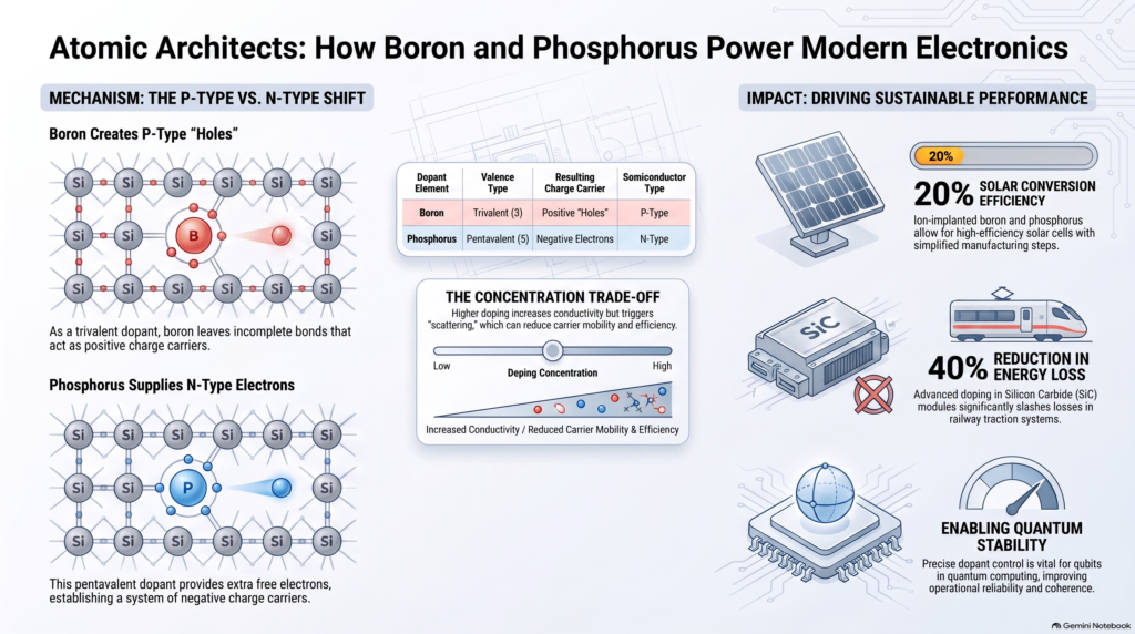
By adding elements like boron or phosphorus, you modify the intrinsic properties of silicon or germanium. Boron, a trivalent dopant, creates holes, resulting in p-type semiconductors, while phosphorus, a pentavalent dopant, contributes additional electrons for n-type semiconductors.
These alterations greatly improve conductivity, enabling the development of advanced electronic devices. Understanding these mechanisms empowers you to manipulate materials effectively, achieving desired electrical characteristics essential for modern technology.
How Does Boron Create P-Type Semiconductors?
Boron creates p-type semiconductors by introducing trivalent atoms into a silicon lattice, where each boron atom forms three covalent bonds with neighboring silicon atoms, leaving one bond incomplete.
This incomplete bonding results in the creation of “holes,” which are positive charge carriers. As you understand the boron role in this process, recognize that these holes enhance the material’s p-type characteristics, allowing for greater conductivity.
The presence of these holes facilitates the movement of charge, making it easier for electrons from adjacent silicon atoms to occupy the vacant states left by boron. Consequently, the doped semiconductor exhibits enhanced electrical properties, characterized by a predominance of positive charge carriers, fundamentally altering its behavior in electronic applications.
How Does Phosphorus Help N-Type Semiconductors Work?
In contrast to boron’s role in creating p-type semiconductors, phosphorus serves as a dopant for n-type materials by introducing pentavalent atoms into the silicon lattice. This addition provides extra electrons, enhancing the n-type properties of the semiconductor.
When you incorporate phosphorus, each atom donates one free electron, considerably increasing the carrier concentration. This surplus of electrons leads to improved conductivity, allowing the material to efficiently transport electrical charge.
The phosphorus role is essential; it establishes a negative charge carrier system that enhances the overall electrical performance of the semiconductor.
You’ll find that n-type semiconductors, with their elevated electron density, are vital in various applications, from transistors to photovoltaic cells, driving modern electronic innovations.
How Do Dopants Like Boron and Phosphorus Affect Carrier Concentration?
Understanding how dopants like boron and phosphorus influence carrier concentration is essential for improving semiconductor performance. When you introduce boron into a semiconductor, it creates holes that serve as positive charge carriers, effectively increasing the p-type carrier concentration.
Conversely, phosphorus adds excess electrons, enhancing n-type carrier concentration. The balance between these dopants directly impacts carrier mobility; higher doping concentrations can lead to increased scattering, limiting mobility and overall efficiency.
Therefore, achieving a favorable doping concentration is critical. Too little dopant may not yield sufficient carriers, while too much can degrade performance due to diminished mobility.
How Does Boron and Phosphorus Doping Modulate Conductivity?
When you introduce boron or phosphorus into a semiconductor, the resulting changes in conductivity are significant and directly linked to the type and concentration of the dopants.
Boron acts as a p-type dopant, creating holes that enhance conductivity through increased positive charge carriers. Conversely, phosphorus serves as an n-type dopant, introducing extra electrons that also promote conductivity. In semiconductor manufacturing, boron and phosphorus function as the active ingredient that enables precise control of electrical conductivity by modifying the concentration of charge carriers. The doping mechanisms involve altering the energy band structure, effectively lowering the energy required for charge carrier movement.
The doping mechanisms involve altering the energy band structure, effectively lowering the energy required for charge carrier movement. As you optimize dopant concentrations, you can achieve a tailored balance between electron and hole concentrations, directly influencing the semiconductor’s electrical properties.
This precision allows you to manipulate conductivity, enabling the design of high-performance electronic devices.
REAL-WORLD APPLICATIONS OF BORON AND PHOSPHORUS
In my work analyzing green chemistry and automated process controls, I often look at semiconductor doping through the lens of efficiency and trade-offs. It’s easy to think that adding more dopant automatically yields better performance, but the physical reality inside the crystal lattice is far more nuanced. When you crank up the concentration of boron or phosphorus, you increase charge carriers, yes but you also introduce ionic scattering. That scattering directly degrades carrier mobility, creating heat and energy loss.
Achieving the perfect balance in p-n junctions is what makes breakthroughs in green technology possible. Take high-efficiency photovoltaic cells, for instance: using techniques like ion implantation for precise boron and phosphorus profile tuning is dramatically reducing manufacturing steps while boosting solar energy conversion. We see the exact same principles applied in wide-bandgap power modules that drive electric traction systems and smart grid infrastructure.
From my perspective, mastering these precise chemical mechanisms is our best lever for slashing “grey energy” costs during manufacturing and maximizing energy savings during decades of operation. It proves that smart atomic-level engineering directly fuels large-scale environmental stewardship.
Boron and phosphorus dopants play a vital role in advancing the semiconductor industry by enhancing the performance of electronic devices. In semiconductor production, doping is the intentional introduction of impurities into an intrinsic (undoped) semiconductor for the purpose of modulating its electrical, optical and structural properties. The doped material is referred to as an extrinsic semiconductor.
Their ability to fine-tune conductivity directly contributes to the development of energy-efficient technologies, reducing power consumption in applications ranging from smartphones to renewable energy systems.
Understanding these real-world applications highlights the importance of precise doping strategies in achieving ideal semiconductor functionality.
Semiconductor Industry Advancements
As the semiconductor industry evolves, the strategic use of boron and phosphorus dopants has become vital for enhancing device performance and functionality.
In quantum computing, these dopants fine-tune the electrical properties of semiconductors, enabling the creation of qubits with improved coherence times and operational reliability. The precision with which boron and phosphorus are introduced allows for tailored electronic characteristics, essential for scalable quantum architectures. These semiconductor technologies are often integrated with samarium cobalt magnets in high-performance electronic systems that require exceptional magnetic stability and reliability. Additionally, in solar cells, the incorporation of these dopants enhances charge carrier mobility and increases energy conversion efficiency.
Additionally, in solar cells, the incorporation of these dopants enhances charge carrier mobility and increases energy conversion efficiency. By optimizing the p-n junctions through controlled doping, manufacturers can greatly boost the overall performance of photovoltaic cells, positioning themselves at the forefront of renewable energy advancements.
Your mastery of these materials is key to driving innovation forward.
Energy Efficient Technologies
The integration of boron and phosphorus in energy-efficient technologies showcases their critical role in optimizing performance across various applications. Doping unlocks silicon’s innate utility by actively controlling its conductive properties. Undoped silicon is rarely used in devices due to its low conductivity and limited functionality. Through doping, we can precisely modulate its properties, enabling revolutionary electronic technologies.
These dopants enhance electrical properties, driving energy conservation strategies and sustainable semiconductor innovations. You can expect to see:
- High-Efficiency Solar Cells: Boron and phosphorus improve charge carrier mobility, maximizing energy conversion rates. These same semiconductor doping principles also support the development of lithium-ion battery active materials, where precise control of electrical conductivity enhances energy storage performance and charging efficiency.
- Advanced LED Lighting: These dopants enable lower power consumption while delivering superior luminosity and longevity.
- Smart Grids: Enhanced semiconductor performance leads to efficient energy distribution and reduced losses.
How Does Carrier Concentration Impact Semiconductor Performance?
Understanding how carrier concentration influences semiconductor performance is essential for optimizing electronic device functionality. Higher carrier concentration typically enhances electrical conductivity, allowing for efficient current flow.
However, this comes at a cost—when you increase carrier concentration excessively, it can lead to decreased carrier mobility due to increased scattering events. This scattering impairs the ability of carriers to traverse the semiconductor, limiting overall performance.
Striking the right balance is vital; you want sufficient carrier concentration to boost conductivity while maintaining high mobility for robust performance.
RELATED STUDIES ABOUT DOPANTS IN SEMICONDUCTOR MANUFACTURING BORON PHOSPHORUS
In conclusion, boron and phosphorus play essential roles in semiconductor doping, fundamentally altering electrical properties. Remarkably, doping can increase carrier concentration by up to 10^20 carriers per cubic centimeter, greatly enhancing conductivity. This modulation of carrier dynamics directly impacts device performance, allowing for tailored applications in electronics. As you explore semiconductor technology, understanding these dopants’ effects is vital for optimizing performance in real-world applications, from transistors to solar cells.
Synthesis of an immobilizable p-dopant and covalent binding onto a polymeric semiconductor
This study addresses a fundamental challenge in the field of organic electronics: the instability of doped layers caused by the migration of mobile dopant counterions. While p-type doping is essential for enhancing the electrical conductivity of organic semiconductors (OSCs), conventional dopants—including powerful radialene-based oxidants—are typically small, diffusible species. Under thermal stress or external electric fields, these mobile counterions can redistribute, leading to device degradation and preventing the formation of stable, sharp p-n junctions.
Key Innovation: Covalent Dopant Immobilization
Researchers developed a novel strategy to chemically anchor a state-of-the-art p-type dopant directly onto a polymeric semiconductor backbone. This covalent binding ensures that neither the dopant molecules nor their corresponding counterions can drift during device operation.
- Dopant Design: An azido-functionalized, radialene-based dopant (CN5HexN3-CP) was synthesized. To preserve its high electron affinity, nitrile groups were strategically replaced with ester groups, which also enhanced the molecule’s solubility and provided a handle for covalent attachment.
- Immobilization Strategy: Due to the extreme reactivity of the neutral dopant, it was introduced to alkyne-functionalized carbazole polymers in its reduced, inert (dianionic) form. Attachment was achieved using both thermal Huisgen cycloaddition and copper-catalyzed azide-alkyne cycloaddition (CuAAC) reactions.
- Activation: Once successfully immobilized, the dopant was activated through controlled oxidation using an external agent (NOSbF_{6}), allowing for the formation of partial charge-transfer interactions while keeping the dopant residues firmly anchored.
Performance and Implications
- Retention of Properties: Cyclic voltammetry confirmed that the immobilized dopant retains its intrinsic redox properties, verifying that the chemical functionalization does not compromise its electrochemical activity.
- Structural Stability: The study demonstrates a proof-of-concept for creating stable, chemically defined doping profiles. By immobilizing both the dopant and the polymer matrix, counterion migration is suppressed.
- Advanced Crosslinking: The remaining unreacted azide groups on the polymer backbone allow for additional crosslinking, further stabilizing the semiconductor layers against mechanical and solvent-induced degradation.
Conclusion
This work marks the first demonstration of covalently binding a high-oxidizing p-dopant to a polymer semiconductor. By suppressing counterion migration, this approach provides a robust framework for localized charge stabilization, serving as a critical step toward the fabrication of stable p/n junctions and more reliable multilayer organic electronic devices.
| REFERENCE: Simon Enders, Roman Tkachov, Anton Kiriy, Enrique Caldera-Cruz, Brigitte Voit, Synthesis of an immobilizable p-dopant and covalent binding onto a polymeric semiconductor, Synthetic Metals, Volume 319, 2026, 118137, ISSN 0379-6779, https://doi.org/10.1016/j.synthmet.2026.118137. (https://www.sciencedirect.com/science/article/pii/S0379677926000652) |
High quality ion implanted boron emitters in an interdigitated back contact solar cell with 20% efficiency
This study reports the fabrication of interdigitated back contact (IBC) silicon solar cells using ion implantation for all doped areas, achieving a conversion efficiency of 20%. This represents the highest efficiency ever reported for an ion-implanted solar cell.
Strategic Context and Challenges
The interdigitated back contact (IBC) architecture is the highest-efficiency solar cell technology currently in mass production. However, its commercial adoption has been limited by the manufacturing complexity of traditional diffusion-based doping, which requires multiple patterning and process steps.
The Ion Implantation Solution
The researchers utilized a “Precision Patterned Implant” (PPI) technology developed by Varian Semiconductor Equipment Associates. This approach offers several key advantages:
- Process Simplification: Ion implantation allows for patterned doping in a single step.
- Manufacturing Efficiency: By using complementary shadow masks during the ion implantation process, the researchers eliminated 9 process steps compared to the baseline diffusion-based manufacturing flow.
- High Throughput: The Solion ion implanter used in this study is capable of processing 1,100 wafers per hour, meeting the throughput requirements of modern photovoltaic (PV) production lines.
Technical Highlights
- Annealing and Passivation: A single, unified thermal annealing step was employed to simultaneously activate the implanted dopants, repair implantation-induced crystal damage, and grow a passivating thermal oxide layer.
- High-Quality Emitters: Lifetime tests using the Quasi-Steady-State Photoconductance (QSSPC) technique confirmed superior emitter quality, with saturation current densities as low as 20{ fA/cm}^2 for boron-doped emitters and phosphorus-doped back surface fields.
- Performance: The fabricated cells reached efficiencies of up to 20%, with the best cell showing a high open-circuit voltage (V_{oc}) of 650.1 mV and a short-circuit current density (J_{sc}) of $40.5{ mA/cm}^2.
Conclusion
The study demonstrates that ion implantation is a viable, high-performance alternative to traditional diffusion methods for IBC cell production. The process simplification offered by PPI technology could reduce costs and improve manufacturing yields while maintaining high conversion efficiencies, thereby contributing to the broader goal of reducing the levelized cost of electricity (LCOE) in the PV industry.
| REFERENCE: Nicholas Bateman, Paul Sullivan, Christian Reichel, Jan Benick, Martin Hermle, High quality ion implanted boron emitters in an interdigitated back contact solar cell with 20% efficiency, Energy Procedia, Volume 8, 2011, Pages 509-514, ISSN 1876-6102, https://doi.org/10.1016/j.egypro.2011.06.174. (https://www.sciencedirect.com/science/article/pii/S1876610211016833) |
Life-cycle energy demand comparison of medium voltage Silicon IGBT and Silicon Carbide MOSFET power semiconductor modules in railway traction applications
This study presents the first life-cycle energy assessment (LCA) based on realistic manufacturing data from a power semiconductor fab for both Silicon (Si) Insulated-Gate Bipolar Transistor (IGBT) and Silicon Carbide (SiC) Metal-Oxide-Semiconductor Field-Effect Transistor (MOSFET) technologies. The analysis focuses on 3.3 kV/450 A “LinPak” modules used in railway traction applications.
Key Findings
- Manufacturing Phase (Grey Energy): While SiC technology requires 2.6–3.8 times more energy per wafer area to manufacture due to more complex front-end processing and higher temperatures, the total energy demand per module is lower for SiC.
- Energy Efficiency: Because SiC devices offer significantly higher power density, a much smaller chip area (10 cm² vs. 40.56 cm²) is required for the same current rating (450 A). Consequently, SiC power modules exhibit 1.1–1.6 times lower “grey energy” (total manufacturing energy) compared to Si modules.
- Use-Phase Dominance: The energy consumed during the manufacturing phase is negligible (less than 0.3%) compared to the energy consumption during the 30-year operational use-phase.
- Energy Savings: Simulations based on realistic suburban railway drive cycles demonstrate that SiC technology can save approximately 40% of the energy losses compared to Si IGBT modules. Over a 30-year operational lifetime, substituting Si modules with SiC technology results in an estimated energy saving of 24 MWh per module.
Implications
- Environmental and Economic Impact: The use-phase energy savings far outweigh the higher manufacturing energy required for SiC wafers. At current electricity prices, this substitution is financially advantageous, with potential cost savings ranging from 1,120 € to 9,364 € per module over a 30-year lifetime, depending on energy prices.
- Industry Baseline: This research provides a critical baseline for LCA practitioners and industry decision-makers to evaluate the environmental implications of wide-bandgap (WBG) semiconductors.
- Future Outlook: With the expected increase in railway electricity costs and further maturity of SiC technology, SiC MOSFETs are poised to become the mainstream choice for high-efficiency railway traction systems.
| REFERENCE: Lucas Barroso Spejo, Innocent Akor, Munaf Rahimo, Renato Amaral Minamisawa, Life-cycle energy demand comparison of medium voltage Silicon IGBT and Silicon Carbide MOSFET power semiconductor modules in railway traction applications, Power Electronic Devices and Components, Volume 6, 2023, 100050, ISSN 2772-3704, https://doi.org/10.1016/j.pedc.2023.100050. (https://www.sciencedirect.com/science/article/pii/S2772370423000184) |
CONCLUSION
Wrapping up, it’s clear that boron and phosphorus dopants remain the workhorses of semiconductor manufacturing, but their applications are evolving faster than ever. Whether we are discussing conventional silicon wafers, flexible organic electronics where chemical drift must be suppressed, or high-performance quantum computing architectures, the ability to control carrier dynamics at the atomic level is paramount.
To me, the most exciting part of this field is seeing how automated lab techniques, advanced process modeling, and computational chemistry are accelerating how we design these doped materials. As we demand higher efficiency from our data centers, renewable energy systems, and daily consumer devices, our approach to semiconductor doping must continue to evolve toward cleaner, lower-impact manufacturing workflows.
Fine-tuning electron and hole concentrations isn’t just about raw computing power, it’s about creating a sustainable foundation for next-generation hardware. If we can pair precise dopant control with eco-friendly chemical processing, the semiconductor industry won’t just keep up with Moore’s Law, it will actively drive the global clean energy transition.